TD - Combinatorial Logic
Overview
Setup
In order to do this exercise, you need to download the archive with the logisim circuits. Save it somewhere in your home directory. Open a terminal and change to the directory where you just saved the archive. Then type the following commands:
tar xzf td-logisim.tar.gz
cd td-logisim
If there are any error messages in the terminal, ask your teacher for help.
The Multiplexer
Exercise: Build a multiplexer ciruit using basic logic gates (AND, OR, NOT, etc).
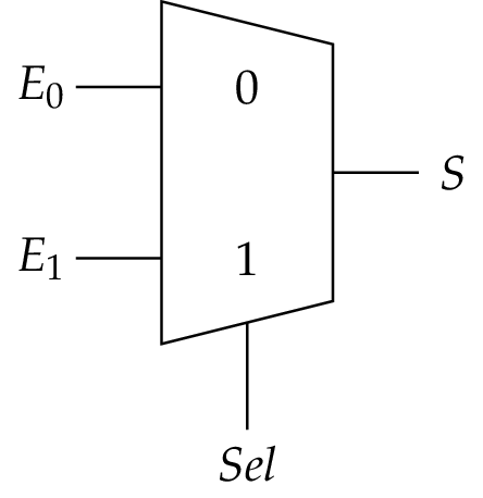
First draft a circuit with paper and pencil. Remember the ciruit equation from the lecture:
\[S = \overline{Sel}\cdot E_0 + Sel\cdot E_1 \]
Now open a terminal and change into the root directory of the extracted archive (see the setup section above). Move into the subdirectory containing the multiplexer exercise and list the files it contains:
cd mux
ls
Here is a short explanation of the files :
- mux-impl.circ: Contains your implementation of the multiplexer circuit. You will need to edit it using logisim.
- mux-spec.circ: Contains a correct multiplexer circuit (in other words, the specification for this exercise), using logisim's circuit library.
- mux-tb.circ: Contains a test bench, i.e. a circuit driving a multiplexer with different inputs in order to observe its behavior.
- Makefile: Contains rules that can be evoked from the command line in order to simulate your circuit and display the results.
The only file that you need to change is mux-impl.circ. But let's start a simulation first. Switch back to the terminal and type
make
This command will read the first rule in the Makefile and try to execute it. In this case, it will simulate the test bench with both the specification and your implementation, generate a waveform file (a timing diagram) and start the program GTKWave to show the waveform. This is what you should see:
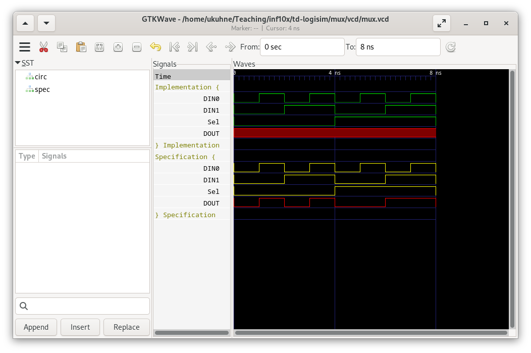
All the subsequent exercices work in a quite similar way, so let's take a minute to inspect the timing diagram. On the left hand side of the window, you can explore all the signals of the two circuits, which are named circ (your implementation) and spec (the correct circuit). In this case (and not surprisingly) they have the same interface. If necessary, you can add signals from the list on the left to the waveform on the right by right-clicking on them.
On the right hand side, you see the waveform of the simulated test bench. Time is progressing from left to right. There are two parts: Implementation shows your circuit's behavior, and Specifciation shows the expected behavior. Note that the inputs (DIN0, DIN1, and Sel) are identical in both cases, this is how a testbench actually works. Here, the testbench exhaustively simulates all (eight) possible input combinations. The only difference between the specification and the implentation part is the outputs. As you can see, there is just a red bar where the DOUT of your implementation should be. This means that the value is unknown. The reason is simply that the circuit does not have an implementation. Let's fix this.
Close the GTKWave window and switch back to the terminal. Type in the following command in order to open the implementation in logisim:
logisim mux-impl.circ &
Note that the little ampersand (&) at the end of the line will start logisim in the background, such that you can still enter new commands in the terminal. You should see something like this:
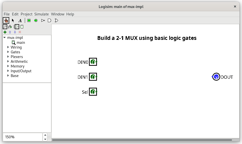
Let's have a quick look at logisim. On the left hand side, you see the current circuit library. For this exercise, the only thing you need is the Gates category. Above is the tool bar. Besides shortcuts for the most frequently used logic gates, there are two important tools that you should understand:
- The hand tool is used to change the values of the inputs in the circuit.
- The pointer tool is used to edit the circuit.
In the circuit view on the right hand side, you see the (empty) circuit. There is only the inputs (rectangular signals with connection points on the right) and the output (round signals with connection points on the left).
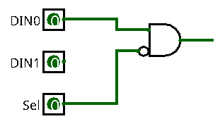
Let's build our first gate. Select the pointer in the tool bar. Choose an AND Gate from the Gates library or click on the AND gate in the tool bar. Then click somewhere in the circuit view to place the gate. You will see the properties of the newly created gate on lower left of the window. Perform the following actions:
- Change the Gate Size to Narrow
- Change the Number of Inputs to 2
- Set Negate 2 to Yes, this will add a small circle to the lower input
- Connect DIN0 to the upper gate input
- Connect Sel to the lower gate input
The result should look like this:
Congratulations, you just created your first gate! Now complete the exercise as follows:
- Create a second AND gate, without negation on the inputs
- Connect DIN1 and Sel to its inputs
- Create an OR gate with 2 inputs
- Connect the outputs of the two AND gates to its inputs
- Connect its output to DOUT
The result should look like this:
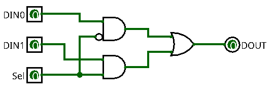
That's it.
Note: Be careful not to delete input or output signals of the circuit! Unfortunately, there is a bug in logisim: Even if you undo (ctrl-Z) the deletion of an input or output, this might break the connections of the circuit within the test bench, and you will get errors or wrong results in the simulation. If this happens, ask a teacher to help you. It might be necessary to restore the original file from the archive to "fix" this problem.
You can now do some basic simulations: Switch to the hand tool and click on the inputs in order to toggle their value. You should be able to observe the output value changing in turn. In order to check if this implementation is correct for all possible input values, switch back to the terminal and type
make
If everything goes fine, this will once again open the waveform viewer with the new waveform:
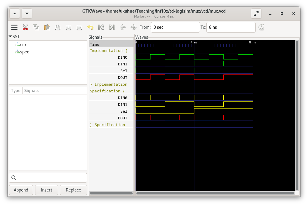
Note that now the waveform of DOUT is identical for both the specification and the implementation.
Building a Subtractor
In the lecture, we have seen the full adder circuit:
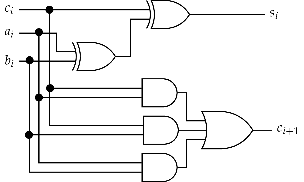
In the same way, we would like to construct a full subtractor, i.e. a circuit that performs one elementary subtraction with incoming carry (also called borrow for subtraction).
Question 1: Show that for subtraction, the carry has negative sign.
In the following, we will use a Boolean value to encode the value of the carry, 0 corresponding to 0 and 1 corresponding to -1.
Our circuit will have the following interface:
- Operand inputs \(A\) and \(B\)
- Incoming carry \(C_{in}\)
- Outgoing carry \(C_{out}\)
- Difference output \(D\)
Question 2: Establish the arithmetic equation connecting the inputs to the outputs.
Question 3: Fill in the truth table relating inputs and outputs:
| \(A\) | \(B\) | \(C_{in}\) | \(C_{out}\) | \(D\) |
|---|---|---|---|---|
| 0 | 0 | 0 | ||
| 0 | 0 | 1 | ||
| 0 | 1 | 0 | ||
| 0 | 1 | 1 | ||
| 1 | 0 | 0 | ||
| 1 | 0 | 1 | ||
| 1 | 1 | 0 | ||
| 1 | 1 | 1 |
Question 4: Establish the Boolean equations for te output signals.
Question 5: Draw a circuit implementing the full subtractor. Compare its structure to the full adder circuit.
In order to test your circuit, there is a testbench in the source archive. Switch to the terminal, move to the root folder of the extracted archive and execute the following commands:
cd sub
logisim sub-impl.circ &
Complete the circuit and type make to simulate it.
The Adder/Subtractor
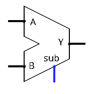
Exercise: Build an arithmetic operator that allows to compute either the sum or the difference between two numbers A and B, given as signed 8 bit integers.
Here are some additional constraints and assumptions:
- The circuit has an additional input sub to indicate wether to perform addition (sub = 0) or subtraction (sub = 1).
- The output of the operator is named Y and has 8 bits
- We will ignore any potential overflow
Question 1: Using pencil and paper, draft a first solution using an adder and subtractor (on 8 bits) and any additional circuit element you consider useful.
This solution is correct but not optimal regarding size (the number of logic gates used). We will build a second solution using the properties of the two's complement representation.
Question 2: Remember the equation used to obtain the (arithmetic) negation of a given number in two's complement.
Question 3: Show that we can implement the adder/subtractor using only one 8 bit adder and an additional operator that computes the bit-wise complement of a two's complement number.
Question 4: Which is the logic operation that allows to select a signal or its complement, depending on a control signal? Extrapolate your solution to 8 bits.
Question 5: Using the above results, propose a new optimized circuit for the adder/subtractor.
There is a testbench in the circuit archive for this exercise. Switch to the subfolder addsub and open the circuits:
cd addsub
logisim addsub-spec.circ addsub-impl.circ &
The specification corresponds to the first solution: two operators and a multiplexer. It is up to you to create the second implementation in the file addsub-impl.circ. In order to check your solution, switch to the terminal and type
make
Optional: Building an Arithmetic-Logic Unit
If you want to go further, you can do this optional exercise. It also serves for the lab exercise on building a RISC-V processor
Introduction
During the previous exercise, we have constructed an (optimised) adder/subtractor, for which we can select the performed operation with an input control signal. This is already quite nice. In this exercise however we would like to add even more operations, generalising our adder/subtractor to an Arithmetic-Logic Unit (ALU). As we will see later in the lecture, the ALU is a central component in every processor. It does an important part of the actual work when executing a program: adding or subtracting numbers, comparing values, shifting bits to the left or to the right, bit-wise logic operations etc.
Specification
How does such an ALU look like? We will keep the interface simple: There are two data inputs and , both representing 8 bit signed integers, and a single data output , also an 8 bit signed integer. Instead of a single control input, we have a 3 bit input , which selects among eight different operations:
| Name | Operation | Description | |
|---|---|---|---|
| 0 | ADD | Signed addition | |
| 1 | SLL | Left shift by positions | |
| 2 | SLT | Set less than | |
| 3 | SUB | Signed subtraction | |
| 4 | XOR | Bit-wise exclusive or | |
| 5 | SRL | Right shift by positions | |
| 6 | OR | Bit-wise or | |
| 7 | AND | Bit-wise and |
Addition and subtraction should be obvious. For the three bit-wise logic operations XOR, OR, and AND, the -ith bit of the output results from the respective logic operation between the -th bits of the inputs.
For left or right shifting, the second input represents the shift amount, i.e. the number of positions that the input is shifted. The direction corresponds to the bit order where the most significant bit (MSB) is on the left and the least significant bit (LSB) is on the right. Left shifting will shift out the most significant bits and fill up the least significant bits with zeros. Right shifting will shift out the least significant bits and fill up the most significant bits with zeros. Since we interpret the input as an unsigned integer (the shift amount), only the lower three bits of should be used, allowing for shift amounts between zero and seven.
Finally, the SLT operation compares two signed integers. If is less than , the output will be (i.e. only the LSB is one and the remaining bits are zero), otherwise the output will be .
Implementation
During the exercise on building an adder-subtractor, the goal was to create a combinatorial circuit optimized for its area: We found out that adding and subtracting could be done by a shared adder circuit, and switching the inputs depending on the requested operation. In this homework, the only goal is functional correctness, i.e. we do not care about the number of gates needed to build the final circuit. This means for example that you can use two separate operators for addition and subtraction without feeling bad about it.
As a starting point, we provide a circuit template and a testbench. Go to the alu subdirectory of the archive and open the file alu.circ:
cd alu
logisim alu.circ &
Note that for each of the eight operations (including shifting and comparison), there is a pre-defined component available in the LogiSim library. Feel free to explore the available components and to instantiate them in your implementation.
Testing your ciruit
In order to run the tests, execute the following command:
make
Do not forget to save your current implementation before running the tests. You should see a wave trace coming up like this:
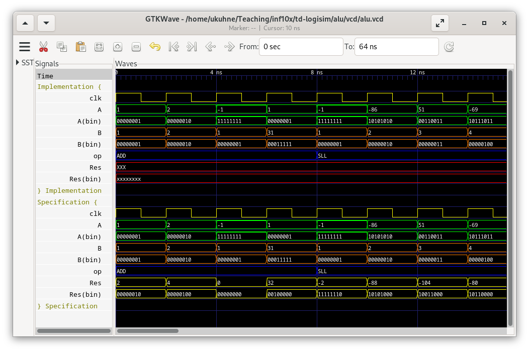
In the trace, the input and output signals and are shown twice, once in binary format and once as signed integers. It's the same signals. Even if the circuit is combinatorial, there is a clock signal. It is only used to generate the test sequence. There are four tests for each of the eight arithmetic and logic operations. Your goal is to reproduce the exact same results for all of the tests (compare between implementation and specification).